 Preconditioning of Nonhermetic Surface Mount Devices Prior to Reliability Testing参考标准:JESD22-A113F 一, Introduction The typical use of surface mount devices (SMD) involves subjecting the SMDs to elevated temperatures during board assembly, which combined with moisture in the package can induce internal package damage that could be a reliability concern. Preconditioning of SMD packages is used to simulate the effects of board assembly on moisturized packages, prior to reliability testing. This allows reliability testing at the component level on as shippable products with a board assembly simulation. During preconditioning, test samples are subjected to temperature cycling (optional), dry bake, moisture soaking, solder reflow simulation, flux, rinse, dry, and electrical test before reliability testing. 板级贴装芯片的时候,需要考虑到封装中的湿气可能会到导致封装damage,这是可靠性需要重点考虑的。SMD的预处理用来模拟可靠性测试前潮湿封装的板级组装。这样可以在器件层面做可靠性测试。预处理过程中,测试样品会经历温度循环(可选项),干燥烘烤,吸湿,焊锡回流焊模拟,溶解,冲洗,干燥和可靠性测试前的电学测试。 二,Scope This Test Method establishes an industry standard preconditioning flow for nonhermetic solid state SMDs that is representative of a typical industry multiple solder reflow operation. These SMDs should be subjected to the appropriate preconditioning sequence of this document by the semiconductor manufacturer prior to being submitted to specific in-house reliability testing (qualification and reliability monitoring) to evaluate long term reliability (which might be impacted by solder reflow). 预处理需要按照正确的顺序进行,预处理后安排后面的长期可靠性测试。 NOTE: Correlation of moisture-induced stress sensitivity (per J-STD-020 and JESD22-A113) and actual reflow conditions used are dependent upon identical temperature measurement by both the semiconductor manufacturer and the board assembler. Therefore, it is recommended that the package temperature at the top center of package be determined during assembly board reflow profile setup, to ensure that it does not exceed the temperature at which the components are evaluated, based on package thickness and volume as stated in IPC/JEDEC J-STD-020. 三 Apparatus 3.1 Moisture chamber temperature Moisture chamber(s) capable of operating at 85 °C/85% RH, 85 °C/60% RH, and 30 °C/60% RH. Within the chamber working area, temperature tolerance must be ±2 °C and the RH tolerance must be ±3% RH. A chamber with 60 °C/60% RH capability is optional for accelerated soak conditions (See J-STD-020). 可以控制温度湿度的chamber,能够运行在85 °C/85% RH, 85 °C/60% RH, and 30 °C/60% RH条件下。chamber中的温度误差要在±2 °C以内,湿度误差在±3% RH以内。60 °C/60% RH的控制能力是可选项,这个条件是为了加速吸湿用的。 3.2 Solder reflow equipment a) (Preferred) - Full Convection reflow system capable of maintaining the reflow profiles required by this standard. 能够实现完全空气对流的reflow设备,能够维持需要的reflow profiles的设备 b) Infrared (IR)/Convection solder reflow equipment capable of maintaining the reflow profiles required by this standard. It is required that this equipment use IR to heat only the air and not directly impinge upon the SMD Packages/devices under test. 红外模拟reflow设备,可以维持需要的reflow profile。这个设备使用的是红外线对空气加热,而不是直接对SMD器件进行直接加热。 NOTE The moisture sensitivity classification test results are dependent upon the package body temperature (rather than the reflow carrier and or package terminal temperature). 湿敏等级分类的测试结果取决于芯片封装体的温度,而不是reflow carrier或者封装端的温度 3.3 Optical microscope Optical Microscope (40x for external visual exam). 光学显微镜 3.4 Electrical test equipment Electrical test equipment capable of performing room temperature dc and functional tests. ATE测试设备 3.5 Bake oven Bake oven capable of operating at 125 +5/-0 °C. 误差在125 +5/-0 °C的烘烤箱 3.6 Temperature Cycle Chamber Temperature Cycle Chamber capable of operating, as a minimum, over the range of (-40 +0/-10) °C to (60 °C +10/-0) °C per JESD22-A104. This equipment is only required if optional Step 4.3 is used. 温度循环chamber,至少可以运行在(-40 +0/-10) °C to (60 °C +10/-0) °C 四, Test procedure Using similar components, it is recommended that the moisture sensitivity level (MSL), per JSTD-020, be determined before starting the preconditioning sequence to establish which moisture soak condition is appropriate, i.e., likely to pass. If the MSL level is not known then other relevant moisture evaluation data may be consulted, or an arbitrary selection may be made. Multiple moisture soak conditions can also be run to determine a passing level. However, the soak condition used must be consistent with the floor life information in IPC/JEDEC J-STD-020. 需要根据芯片湿敏等级来决定吸湿的条件 如果芯片的湿敏等级未知,需要收集其他数据。 Reflow requirements are provided for both SnPb and Pb-free conditions and should be used based on the intended end use of the component. The same package may have different MSL levels depending on whether the SnPb or Pb-free reflow is used. reflow需要提供SnPb and Pb-free两种条件。SnPb and Pb-free封装芯片使用的reflow条件是不同的。 At all times the test parts should be handled using proper ESD procedures in accordance with JESD625. 整个预处理过程中芯片的处理应该要符合ESD防护需求 Refer to Annex A for the typical test flow. NOTE If the preconditioning sequence is being performed by the semiconductor manufacturer, steps 4.1, 4.2, and 4.4 are optional since they are the supplier's risks. If the preconditioning sequence is being performed by the user, steps 4.7 through 4.9 are optional. 如果是生产商做的预处理,那么4.1, 4.2, and 4.4是可选项,因为这些是供应商的risk。 如果预处理是用户来做,那么4.7到4.9是可选项。 4.1 Initial electrical test Perform electrical and/or functional test to verify that the devices meet the room temperature data sheet specification. Replace any devices that fail to meet this requirement. 预处理前需要进行电学和功能测试,所以进预处理的芯片要全部pass电学和功能测试 4.2 Visual inspection Perform an external visual examination under 40X optical magnification to ensure that no devices with external cracks or other damage are used in this test method. If mechanical rejects are found, corrective action must be implemented in the manufacturing process and a new sample must be drawn from product that has been processed with the corrective action. 需要进行外观检验,确保进预处理的芯片没有crack或者其他的损伤。 如果发现了机械造成的reject,生产过程中要采取纠正方案进行改正生产,并且芯片需要使用改正生产后的芯片进行预处理测试。 4.3 Temperature cycling Perform five (5) cycles of temperature cycle from -40 °C (or lower) to 60 °C (or higher) to simulate shipping conditions. Acceptable alternative test conditions and temperature tolerances are A through I and L through N as defined in Table 1 of JESD22-A104, Temperature Cycling. This step is optional based on product requirements. 温度循环:5次温度循环,从-40 °C到60 °C,来模拟运输过程中的状况。这个对不同的产品来说,是可选项。 4.4 Bake out Bake the devices for 24 hours minimum at 125 +5/-0 °C. This step is intended to remove all moisture from the package so that it will be “dry.” 烘烤,在125 +5/-0 °C烘烤至少24小时,将芯片中湿气全部bake出去 NOTE This time/temperature may be modified if desorption data on the particular device being preconditioned shows that a different condition is required to obtain a "dry" package. Refer to J-STD-020 for procedures on running absorption and desorption curves. 4.5 Moisture Soak Place devices in a clean, dry, shallow container so that the package bodies do not touch or overlap each other. Submit each sample to the appropriate moisture soak requirements shown in IPC/JEDEC J-STD-020. The moisture soak should be initiated within 2 hours of bake. 吸湿:将芯片放在干净干燥,比较浅的容器中,每个芯片单独放置,与其芯片无接触,无重叠,然后执行吸湿实验,吸湿实验要在烘烤结束后2个小时内执行。 NOTE The moisture soak is optional for devices (Flip Chip die, etc.) where moisture absorption data is available showing the particular device being preconditioned does not absorb moisture. Refer to J-STD-020 for procedures on running absorption and desorption curves. 4.6 Reflow Not sooner than 15 minutes and not longer than 4 hours after removal from the temperature/humidity chamber, subject the sample to 3 cycles, Note 1, of the appropriate reflow conditions. The reflow conditions are defined in IPC/JEDEC J-STD-020. If the timing between removal from the temperature/humidity chamber and initial reflow cannot be met then the parts must be rebaked and resoaked according to 4.4 and 4.5. 芯片从高温高湿chamber中拿出来后,要在15分钟到4小时内安排进行3个循环的reflow。 如果间隔时间大于4小时,需要重新进行bake+吸湿。 NOTE 1 The 3 cycles for the component represent the following: - Cycle 1 - the first pass of a Double-Sided, Double-Pass (DSDP) assembly reflow process. - Cycle 2 - the second pass of a DSDP assembly reflow process. - Cycle 3 - rework of a near neighbor component on the assembly where the component being classified experiences reflow-like temperatures. NOTE 2 If the reflow cycle regimen is not representative for the component being classified, refer to JESD94 for application specific qualification guidance. The sample parts shall be cooled sufficiently (preferably back to room temperature) between reflow cycles so that the reflow temperatures/times of the samples are not affected on the subsequent reflow cycles. reflow cycle之间,芯片应该能够降温到室温,这样reflow的效果不受随后reflow的影响。 Reflow practices shall be sufficient to ensure that all sample parts, in each reflow cycle, will meet the appropriate reflow profile requirements of IPC/JEDEC J-STD-020. Reflow需要确保reflow profile满足相关的要求 Components intended for use in a “Pb-free” assembly process shall be evaluated using the “Pb-free” reflow temperature whether or not the component is Pb-free. Pb-free和有pb的reflow profile是不同的 4.6 Reflow (cont’d) If parts are reflowed in other than the normal assembly reflow orientation (i.e. live bug/dead bug) the damage response should be correlated. The reflow oven should be loaded with the same configuration when running preconditioning as was used to develop the reflow profile. The reflow profiles in IPC/JEDEC J-STD-020 are for classification/preconditioning and are not meant to specify board assembly profiles. Actual board assembly profiles should be developed based on specific process needs and board designs and should not exceed the parameters in IPC/JEDEC J-STD-020. 4.6.1 Solder attachment after reflow If reliability testing is to be performed in a second level configuration, one of the reflow cycles may be used to attach the device to the test board. If the board assembly is to be preformed at a later time then the devices, at the user discretion, can be baked and vacuum sealed until such time that it is solder attached to the test board or facsimile. Since the board attachment replicates a real life process with flux application, reflow and cleaning, steps 4.7 and 4.8 are no longer necessary or mandated prior to submission to reliability stress testing. Flux type shall be documented per section 6. 如果可靠性测试需要在下一级的组装中执行,那么其中的一个reflow cycle需要将芯片贴到测试板子上。 如果板子组装后的测试安排时间比较晚,那么芯片需要bake然后抽真空封口,直到需要的时候再焊接到板子上。 芯片焊接到板子上是一个真正的锡球溶解焊接过程,reflow和清洁,step 4.7和4.8不是必须的。 4.7 Flux application After the reflow solder cycles are completed, allow the devices to cool at room ambient for 15 minutes minimum. Devices shall then be dipped (full body immersion) in an activated water soluble flux at room ambient for 10 seconds minimum. reflow cycle结束后,芯片降温到室温,至少需要15分钟,芯片在室温下全部侵入到活性水溶性助熔剂,持续至少10秒 Ball Grid Array (BGA), Column Grid Array (CGA) and organic substrate Land Grid Array (LGA) packages do not require flux dipping because their typical board application methods do not use liquid fluxes. Steps 4.8 and 4.9 are not required when flux dipping is omitted for these package types. BGA,CGA和LGA不需要熔剂浸渍,因为他们的板子不用液体助熔剂。那么step 4.8和step 4.9就不需要了。 4.8 Cleaning Clean devices externally using multiple agitated deionized water rinses. No waiting time is required between flux application and cleaning. Ensure all flux residuals are completely removed. 使用多次搅拌去离子水冲洗芯片外部。flux和清洗之间不需要等待时间,要确认flux的残留物被完全清除。 助焊剂(flux):在焊接工艺中能帮助和促进焊接过程,同时具有保护作用、阻止氧化反应的化学物质。助焊剂可分为固体、液体和气体。主要有“辅助热传导”、“去除氧化物”、“降低被焊接材质表面张力”、“去除被焊接材质表面油污、增大焊接面积”、“防止再氧化”等几个方面,在这几个方面中比较关键的作用有两个就是:“去除氧化物”与“降低被焊接材质表面张力”。 4.9 Drying Devices should be dried at room ambient prior to submission to reliability testing. 芯片在可靠性测试前需要在常温下做干燥处理 4.10 Final electrical test Submit the devices to electrical and/or functional testing per the room temperature data sheet specification. For the semiconductor manufacturer, this step is optional and may be omitted since it is a supplier's risk. Any valid failures found at this point due to the preconditioning sequence indicate that the device may have been classified in the wrong level or something is substandard with the test devices. Failure analysis should be conducted. If appropriate, this device type should be reevaluated to determine the correct moisture sensitivity level. This would require resubmitting a sample to the correct level preconditioning sequence prior to reliability testing per 5. 五, Applicable reliability tests SMDs should be subjected to the appropriate preconditioning sequence of this document prior to being submitted to reliability tests per JESD47 or the semiconductor manufacturer’s in-house reliability procedures. 六, Summary The following details shall be specified in the applicable procurement document. a) Rev of IPC/JEDEC J-STD-020 used for the reflow profile. b) Number of reflow cycles if other than three. c) Type of flux if other than Step 4.7. d) Reliability tests if other than 5. e) Test conditions and duration of reliability tests in 5. f) Electrical test description, including test temperature(s). 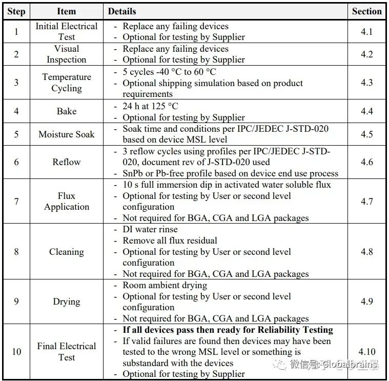 |